■ Example of research topics ■
[ Solar ]
1. 4 junction by wafer bonding /
2. High-speed MOVPE /
3. EL and PL characterization /
4. Thin-film multi-junction (design and light trapping) /
5. 1.15 eV middle cell with MQWs /
6. Theoretical modeling of MQWs (quasi bulk approach and cell design) /
7. WoW /
8. ELO /
9. Dilute nitride MQW
[ Growth ]
1. III-V on Si photo detector /
2. III-V on Si solar cell
[ LED ]
1. Chip-white LED
[ Solar Fuel ]
1. CPV + water electrolysis /
2. CO2 reduction /
3. Semiconductor/electrolyte interface /
4. Polarization-controlled nitride photocathode /
5. Design of energy management system using hydrogen-based power storage
[ Quantum Modeling ]
1. Quantum modeling of insulators
Investigation of growth mechanism of InGaAs microdiscs on Si and application to infrared photodetectors
T. Watanabe Y. Nakano and M. Sugiyama
InGaAs is used as a material for infrared light emission and detection devices. As InGaAs is normally grown on InP substrate, InGaAs devices have problems such as high cost and small area. Growth of III-V layers on a Si substrate can solve such intrinsic problems of InGaAs. Selective area growth (SAG) technique is very attractive for integrating III-V microdiscs monolithically on a Si substrate patterned with SiO2 mask. The three-dimensional feature with small contacting area with Si can help releasing stress stemming from the lattice mismatch between a III-V material and Si, allowing us to obtain high-quality III-V layers on Si. We have been successful in growing InGaAs microdiscs on Si with several micrometers in diameter. Through comprehensive survey of the impact of growth conditions such as partial pressure of source materials and temperature on the shape and atomic content of the microdiscs, we aim at elucidating the mechanism of microdisc growth and the improvement in shape uniformity of the microdiscs. We are implementing p-i-n junction in the InGaAs microdiscs for the application of multi-pixel InGaAs infrared photodetectors integrated with Si circuits.
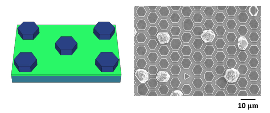
Fig. A schematic and an SEM image of InGaAs microdiscs on Si