■ Example of research topics ■
[ Solar ]
1. 4 junction by wafer bonding /
2. High-speed MOVPE /
3. EL and PL characterization /
4. Thin-film multi-junction (design and light trapping) /
5. 1.15 eV middle cell with MQWs /
6. Theoretical modeling of MQWs (quasi bulk approach and cell design) /
7. WoW /
8. ELO /
9. Dilute nitride MQW
[ Growth ]
1. III-V on Si photo detector /
2. III-V on Si solar cell
[ LED ]
1. Chip-white LED
[ Solar Fuel ]
1. CPV + water electrolysis /
2. CO2 reduction /
3. Semiconductor/electrolyte interface /
4. Polarization-controlled nitride photocathode /
5. Design of energy management system using hydrogen-based power storage
[ Quantum Modeling ]
1. Quantum modeling of insulators
High-efficiency photovoltaic solar cells using Wire on Well structure
S. Saito, T. Kasidit, K Watanabe, Y. Nakano, M. Sugiyma
Multi-junction solar cell holds the highest record efficiency. For 3-junction solar cells, however, the largest bottleneck for the highest efficiency is the absence of the material that satisfies the lattice matching to the substrate material Ge and the bandgap of 1.2 eV that is necessary for current matching among subcells. By using a strain balanced quantum well, in which a narrow-gap absorber InGaAs and a strain-compensating material GaAsP are alternatively stacked, an effective band gap of 1.2 eV is realized keeping effective lattice matching to a Ge substrate. When such a multiple quantum well (MQW) structure is grown on 6-degree offcut GaAs (001) substrate at relatively low temperature, a wavy structure can be obtained with the thickness modulated periodically along an eigenaxis of GaAs. For this Wire on Well (WoW) structure, carrier lifetime is found to be longer and carrier collection efficiency is higher than a planar MQW. Moreover, its wire size can be tailored by growth parameters such as growth time of the wells, making the effective band gap tunable. We aim at obtaining a 1.15-eV-bandgap subcell using such a WoW structure, which can serve as the 3rd cell of a lattice-matched 4-junction cell. Taking advantage of the long carrier lifetime, we also aim at applying a WoW structure to intermediate-band solar cells.
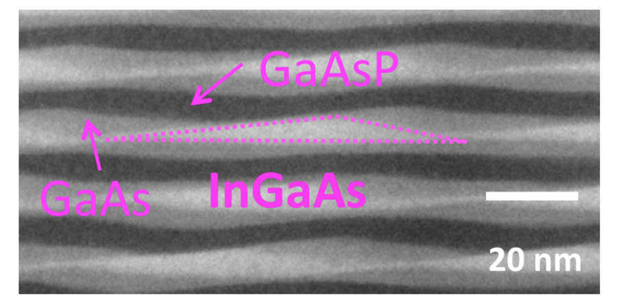
Fig. 1 A cross-sectional TEM image of a Wire on Well (WoW) structure
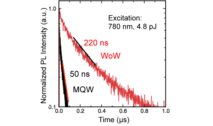
Fig. 2 Comparison of carrier lifetime for WoW and planar quantum wells
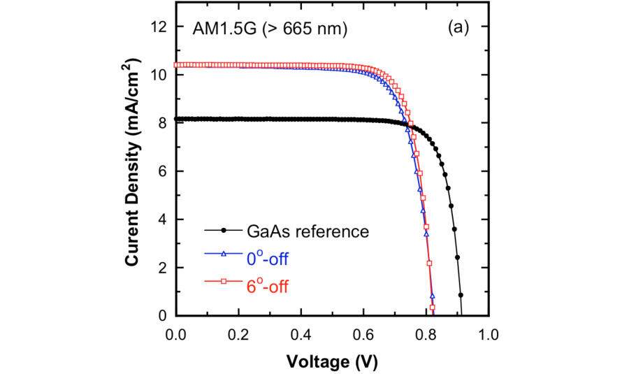
Fig. 3 Comparison of current-voltage characteristics for GaAs single junction cells using WoW and planar quantum wells as log-wavelength light absorber.