■ Example of research topics ■
[ Solar ]
1. 4 junction by wafer bonding /
2. High-speed MOVPE /
3. EL and PL characterization /
4. Thin-film multi-junction (design and light trapping) /
5. 1.15 eV middle cell with MQWs /
6. Theoretical modeling of MQWs (quasi bulk approach and cell design) /
7. WoW /
8. ELO /
9. Dilute nitride MQW
[ Growth ]
1. III-V on Si photo detector /
2. III-V on Si solar cell
[ LED ]
1. Chip-white LED
[ Solar Fuel ]
1. CPV + water electrolysis /
2. CO2 reduction /
3. Semiconductor/electrolyte interface /
4. Polarization-controlled nitride photocathode /
5. Design of energy management system using hydrogen-based power storage
[ Quantum Modeling ]
1. Quantum modeling of insulators
Characterization of the photoelectrode/electrolyte interface with first principles modeling and in situ measurement
M. Sato, K. Fujii (RIKEN), and M. Sugiyama
Microscopic understanding and characterization of semiconductor/electrolyte interface structures are essential for tailoring the properties of photoelectrochemical reactions. In this study, we reveal the semiconductor/electrolyte interface structure with the aid of first principles calculations and in situ measurements. Even though, first principles calculation has become a powerful tool for materials design in many fields, theoretical design of photocatalysts and photoelectrodes has met with limited success. To overcome this problem, we investigate from first-principles, the carrier accumulation processes at the semiconductor/electrolyte interface, which, though usually disregarded, has a large impact on photoelectrochemical reactions. In addition, together with in situ measurements using infra-red or X-rays, the semiconductor/electrolyte interface structure is studied. In the case of GaN/water interface, both atomistic simulations and FTNIR experiments indicate that the interface structure changes under UV radiation. These results underline the importance of the surface-charge-sensitive modeling approach.
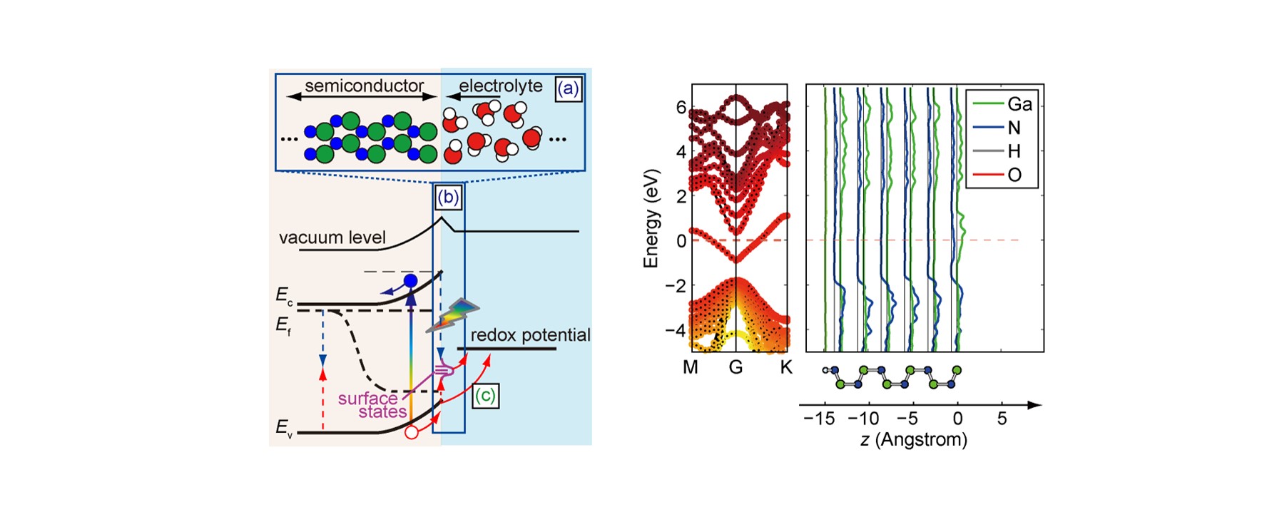
Fig. 1 (left) Schematics of photoelectrode/electrolyte interface: (a) geometric structure, (b) electronic structure, and (c) charge transfer and chemical reactions. (right) Typical electronic structure of GaN surface.