■ Example of research topics ■
[ Solar ]
1. 4 junction by wafer bonding /
2. High-speed MOVPE /
3. EL and PL characterization /
4. Thin-film multi-junction (design and light trapping) /
5. 1.15 eV middle cell with MQWs /
6. Theoretical modeling of MQWs (quasi bulk approach and cell design) /
7. WoW /
8. ELO /
9. Dilute nitride MQW
[ Growth ]
1. III-V on Si photo detector /
2. III-V on Si solar cell
[ LED ]
1. Chip-white LED
[ Solar Fuel ]
1. CPV + water electrolysis /
2. CO2 reduction /
3. Semiconductor/electrolyte interface /
4. Polarization-controlled nitride photocathode /
5. Design of energy management system using hydrogen-based power storage
[ Quantum Modeling ]
1. Quantum modeling of insulators
III-V on Si growth technology for high-efficiency, low-cost tandem solar cells
Boram Kim, T. Okada, M. Sugiyama
The tandem solar cell consisted of III-V compound semiconductor and Si is promising for achieving high energy conversion efficiency and reducing the cell cost. We have proposed a new structure for III-V/Si tandem solar cell with multi-quantum well (MQW) structure, in which MQW extends the absorption edge to longer wavelengths than the property of the host III-V material and achieves current matching between two subcells while minimizing the lattice mismatch between the host III-V material and Si. We are developing crystal growth technology in order to implement the proposed structure. In III-V material growth on Si, it is required to reduce threading dislocations in the III-V layers, which are caused by the mismatch of lattice constant, polarization and thermal expansion coefficient between Si and III-V semiconductors, to below 106/cm2. In this research, in-situ reflectance anisotropy spectroscopy (RAS) is used for crystal quality evaluation and optimizing the growth condition during metal-organic vapor phase epitaxy (MOVPE). We have been successful in the preparation of double step structure, which is mandatory for eliminating anti-phase boundaries in the III-V layer growth on Si, by the preflow of an arsenic precursor and the subsequent annealing in H2 ambient. Dislocation-free GaP is obtained on that Si surface. The next target is the growth of metamorphic buffer in the GaP seed and the growth of MQWs.
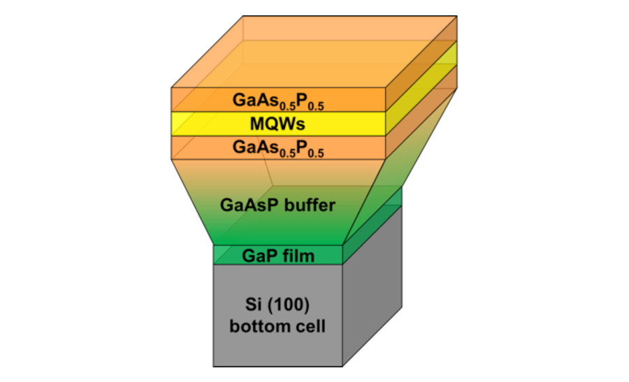
Fig. 1 A schematic of the III-V multiple quantum well (MQW) on Si tandem cell
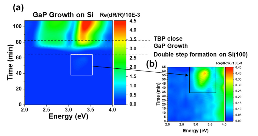
Fig. 2 Surface reflectance anisotropy signal during the growth of GaP on Si.
(a) an entire view and (b) the portion indicating the formation of double steps on Si (100) surface.