■ Example of research topics ■
[ Solar ]
1. 4 junction by wafer bonding /
2. High-speed MOVPE /
3. EL and PL characterization /
4. Thin-film multi-junction (design and light trapping) /
5. 1.15 eV middle cell with MQWs /
6. Theoretical modeling of MQWs (quasi bulk approach and cell design) /
7. WoW /
8. ELO /
9. Dilute nitride MQW
[ Growth ]
1. III-V on Si photo detector /
2. III-V on Si solar cell
[ LED ]
1. Chip-white LED
[ Solar Fuel ]
1. CPV + water electrolysis /
2. CO2 reduction /
3. Semiconductor/electrolyte interface /
4. Polarization-controlled nitride photocathode /
5. Design of energy management system using hydrogen-based power storage
[ Quantum Modeling ]
1. Quantum modeling of insulators
Diluted-N Multiple Quantum Well with Flat Conduction Band Structure for multijunction solar cell
W. Yanwachirakul, N. Miyashita (Okada Lab.), H. Sodabanlu, K. Watanabe, M. Sugiyama Y. Okada (Okada Lab.) and Y. Nakano
A diluted-N (InGaAsN) alloy can be a candidate material for the optimized structure of lattice-match multijunction solar cell on Ge. Because of the unique characteristic of large bowing parameter, the energy gap of this alloy can be decreased to 1.2 eV (for the middle cell of three-junction) and 1.0 eV (for 2nd cell of four-junction) by a small amount of incorporated N.
However, it is difficult to apply this alloy to solar cells since electrons are possibly trapped by the N-related localized states below the conduction band, resulting in inefficient electron transport in this material. In order to prevent electrons from being trapped by these localized states, a novel InGaAs/GaAsN multiple quantum well (MQW) structure has been invented where N-free layer (InGaAs) is placed periodically in between N-containing layers (GaAsN).
In this research, the novel strain-balanced InGaAs/GaAsN MQW with flat conduction band (FCB), without band offset between two materials in the conduction band, has been designed and fabricated. Our up-to-date results confirm that (1) the electron lifetime was increased and (2) the carrier transport could be improved by the FCB MQW compared to the bulk structure in term of carrier collection efficiency (CCE).
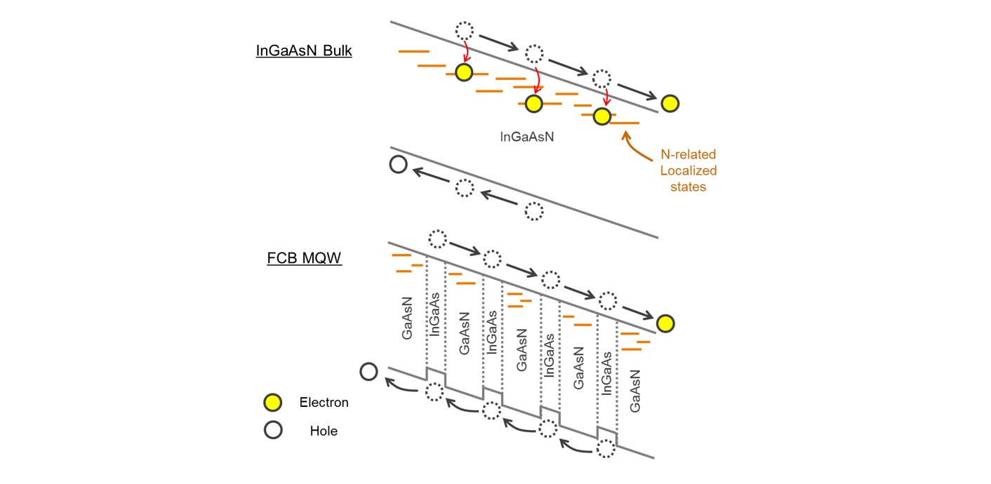
Fig. 1 Electron and hole transport in InGaAsN bulk and InGaAs/GaAsN FCB MQW.
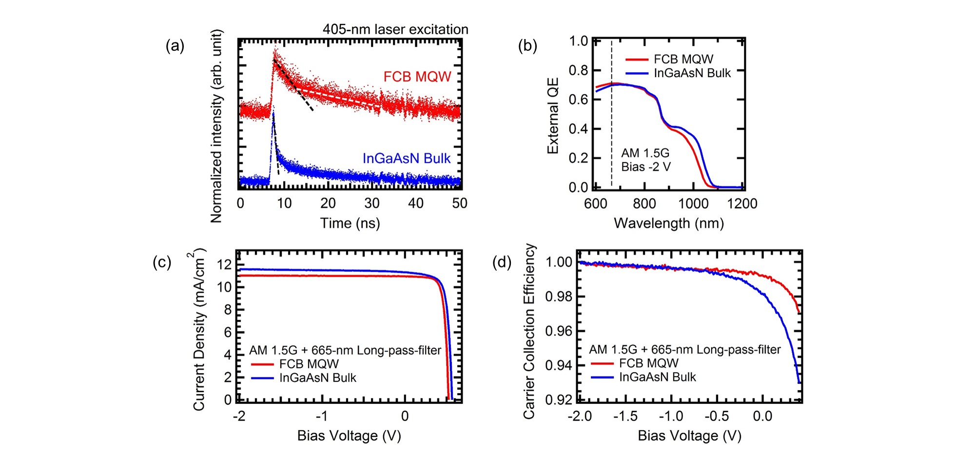
Fig. 2 Comparison of (a) photoluminescence decay time (b) external quantum efficiency (EQE) (c) current-voltage (I-V) characteristic and (d) carrier collection efficiency (CCE) between two single-junction cells using InGaAsN bulk and InGaAs/GaAsN FCB MQW as light absorber, respectively.