■ Example of research topics ■
[ Solar ]
1. 4 junction by wafer bonding /
2. High-speed MOVPE /
3. EL and PL characterization /
4. Thin-film multi-junction (design and light trapping) /
5. 1.15 eV middle cell with MQWs /
6. Theoretical modeling of MQWs (quasi bulk approach and cell design) /
7. WoW /
8. ELO /
9. Dilute nitride MQW
[ Growth ]
1. III-V on Si photo detector /
2. III-V on Si solar cell
[ LED ]
1. Chip-white LED
[ Solar Fuel ]
1. CPV + water electrolysis /
2. CO2 reduction /
3. Semiconductor/electrolyte interface /
4. Polarization-controlled nitride photocathode /
5. Design of energy management system using hydrogen-based power storage
[ Quantum Modeling ]
1. Quantum modeling of insulators
Feasibility of thin-film InGaP/GaAs/InGaAs multi-junction solar cells using light trapping for low-cost and high-efficiency applications
A. G. Reddy, Lin Zhu (ISSP, Univ. Tokyo), Kentorah Watanabe, Hidefumi Akiyama (ISSP, Univ. Tokyo), Yoshiaki Nakano, Masakazu Sugiyama
Very high efficiency solar cells have been achieved using InGaP/GaAs/InGaAs inverse-metamorphic multi-junction technology for both concentrator and non-concentrator applications. To compete with matured silicon-based solar cells in terms of large-scale deployment, the price of the III-V solar cells need to be significantly reduced. One of the ways to achieve the desired LCOE (Levelised Cost of Electricity) is to develop low-cost technology such as substrate reuse and high-speed growth. Reduction of layer thicknesses in III-V cells is another route for cost reduction. One of the focus of our work is to obtain a minimum-thickness design for a InGaP/GaAs/InGaAs 3-junction cell using light trapping technique followed by realistic prediction of efficiency. We have developed a model in which we formulated general absorptivity of multi-junction cells and applied that to simulate absorption spectrum and photo-generated current of each subcell using MATLAB. We then predicted the current-voltage characteristics (and thus cell efficiency) of the multi-junction cells with light-trapping structure using modified detailed balanced model, which takes into account non-radiative carrier recombination and luminescence coupling among subcells as well as the most basic radiative carrier recombination.
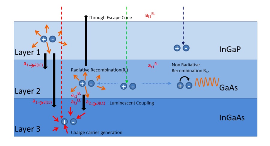
Fig. 1 A schematic depicting major optical processes in a multi junction solar cell including internal and external emission, radiative and non-radiative carrier recombination and luminous coupling. a(2→3) represents absorptivity of subcell 3 for the emission from subcell 2.