■ Example of research topics ■
[ Solar ]
1. 4 junction by wafer bonding /
2. High-speed MOVPE /
3. EL and PL characterization /
4. Thin-film multi-junction (design and light trapping) /
5. 1.15 eV middle cell with MQWs /
6. Theoretical modeling of MQWs (quasi bulk approach and cell design) /
7. WoW /
8. ELO /
9. Dilute nitride MQW
[ Growth ]
1. III-V on Si photo detector /
2. III-V on Si solar cell
[ LED ]
1. Chip-white LED
[ Solar Fuel ]
1. CPV + water electrolysis /
2. CO2 reduction /
3. Semiconductor/electrolyte interface /
4. Polarization-controlled nitride photocathode /
5. Design of energy management system using hydrogen-based power storage
[ Quantum Modeling ]
1. Quantum modeling of insulators
Direct observation of carrier transport dynamics in quantum structures using time-of-flight technique
K. Toprasertpong, M. Asami, A. Delamarre, K. Watanabe, Y. Nakano, and M. Sugiyama
Quantum structures such as quantum wells or quantum wires are promising materials to realize next-generation solar cells, including the applications in multi-junction solar cells, intermediate-band solar cells, and hot-carrier solar cells. To fully extract their potential, we have to gain our understanding of the carrier transport dynamics inside such structures. Carrier transport dynamics so far has been analyzed using indirect measurement methods which have a limitation in understanding the underlying physics. We introduce the “carrier time-of-flight” measurement technique which can directly observe the carrier dynamics including the transport time and velocity inside the quantum structures. This allows us to analyze the carrier transport in the microscopic scale and provides important clues for the theoretical modeling of effective carrier mobility and related phenomena in the quantum structures.
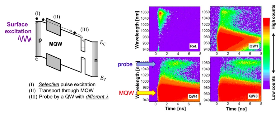
Fig. Carrier time-of-flight measurement technique and example of measurement results.