■ Example of research topics ■
[ Solar ]
1. 4 junction by wafer bonding /
2. High-speed MOVPE /
3. EL and PL characterization /
4. Thin-film multi-junction (design and light trapping) /
5. 1.15 eV middle cell with MQWs /
6. Theoretical modeling of MQWs (quasi bulk approach and cell design) /
7. WoW /
8. ELO /
9. Dilute nitride MQW
[ Growth ]
1. III-V on Si photo detector /
2. III-V on Si solar cell
[ LED ]
1. Chip-white LED
[ Solar Fuel ]
1. CPV + water electrolysis /
2. CO2 reduction /
3. Semiconductor/electrolyte interface /
4. Polarization-controlled nitride photocathode /
5. Design of energy management system using hydrogen-based power storage
[ Quantum Modeling ]
1. Quantum modeling of insulators
Photoluminescence and Electroluminescence characterization of solar cells
A. Delamarre,Hsiang-Hung Huang, K. Watanabe, Y. Nakano, M. Sugiyama
Luminescence is the process by which a semiconductor emits light, when this semiconductor is brought out of equilibrium by an excitation source. The excitation source can be an illumination (in this case the luminescence is called photoluminescence) or an applied electric bias (in this case the luminescence is called electroluminescence), or a combination of both. Measuring the luminescence of a solar cells brings numerous information, such as the quasi-Fermi level splitting, carrier transport, series resistances, defects...[1]. It can also be measured without contact in the case of photoluminescence, so that the method is adapted to industrial production lines.
Our laboratory is currently active on the three following directions:
- - Thanks to an absolute calibration of our luminescence setup, we are able to measure the number of photons emitted by a solar cell. This allows us to determine the cell radiative efficiency, which is a relevant performance indicator of our devices [2].
- - We develop original methods for characterizing the efficiency of the lateral carrier transport, which provides efficiency maps, as displayed in figure b [3]. This measurement can be carried out in single junction as well as multijunction cells, see figure c.
- - Advanced solar cell concepts make use of nanostructured absorbers, containing quantum wells, wires or dots. Therefore, the in-depth carrier transport becomes critical. We have shown that luminescence can reveal such mechanisms [4], and new directions are currently explored to prepare more efficient cells.
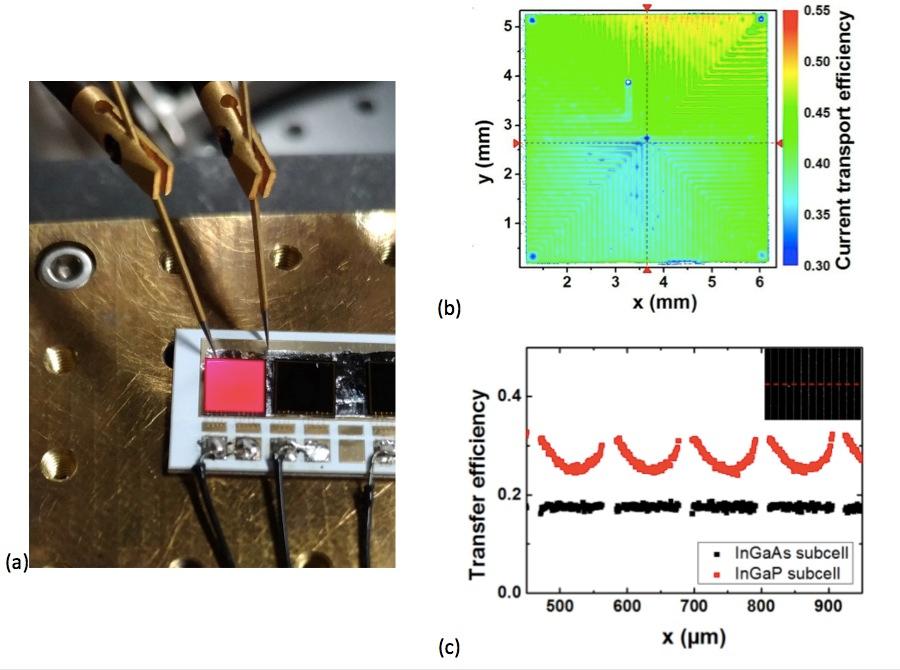
(a) Luminescence emission of a InGaP solar cell at 642 nm. (b) Carrier transport efficiency on a GaAs solar cell, determined from luminescence. (c) Carrier transport efficiency in a multijunction solar cell. The InGaAs and InGaP sub cell can be distinguished [5].
Reference and selected publications:
[1] J.-F. Guillemoles et al., « Material Challenges for Solar Cells in the XXIst century », STAM.
[2] K. Toprasertpong et al., « Electroluminescence-based quality characterization of quantum wells for solar cell applications », J. Cryst. Growth, oct. 2016.
[3] A. Delamarre, L. Lombez, K. Watanabe, M. Sugiyama, Y. Nakano, et J.-F. Guillemoles, « Experimental Demonstration of Optically Determined Solar Cell Current Transport Efficiency Map », IEEE J. Photovolt., vol. 6, no 2, p. 528‑531, mars 2016.
[4] A. Delamarre, Y. Wang, K. Watanabe, Y. Nakano, M. Sugiyama, et J.-F. Guillemoles, « Influence of the host PIN diode material in multi-quantum well solar cells », in Proceedings of the 31st European Photovoltaic Solar Energy Conference and Exhibition, Hamburg, 2015, p. 48.
[5] A. Delamarre et al., « Characterisation of multi-junction solar cells by mapping of the carrier transport efficiency using luminescence emission », in SPIE Proceeding, Physics, Simulation, and Photonic Engineering of Photovoltaic Devices VI, San Francisco, 2017, p. 100990Z.